R&D for Semiconductor
DNF R&D center has been working on development of core materials for semiconductor to meet the needs of customer and
industry since 2003. We have done several joint research and development projects with chip-makers, equipment companies,
and university laboratories successfully. Those achievements and products by continuous and steady R&D efforts helped
global semiconductor industry to develop, and it was the way we could make your life better.
DNF R&D Roadmap (Developed, Developing)
| Wire |
Alpis-3 |
MABOC (Ep-Cu Seed) |
CVD/ALD Cu Precursor |
| Electrode |
TiCl4 / TEMAT / TDMAT / Ru Precursor |
| High-k |
TEMAHf / TEMAZr |
Zr Precursor |
STO/BST/Zr Precursor |
| Low-k |
|
Low-k (CVD) Precursor |
| Gap-Fill |
Polysilazane |
Flowable Oxide Precursor |
| Diffusion Barrier |
TiCl4 |
TDMATi / Ta Precursor |
Ru Precursor |
| Etch Hardmask |
SiN |
1-Hexene/Propylene (ACL) |
SOC Precursor |
| Low Temp. Silicon (DPT) |
|
DIPAS |
ALD SiO2 |
| New Memory |
Ge / Sb / Te / Fe / Co / Ni Precursor |
| Gate Metal |
(CVD) Ni / Co / W Precursor |
ALD Metal |
| TSV |
ALD SiO2 / Ti Precursor / Ta Precursor / CVD Cu |
| |
50nm |
40nm |
30nm |
20nm |
10nm~ |
* CVD : Chemical Vapor Deposition
* ALD : Atomic Layer Deposition
* Ep : Electroplating
* SOC : Spin on Carbon
* ACL : Amorphous Carbon Layer
* DPT : Double Patterning Technology
* TSV : Through Silicon Via
R&D for Display
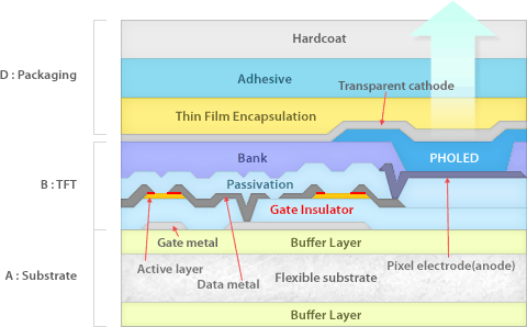
People are getting interested in smartphone and tablet PC, it will be much bigger when they are flexible. DNF R&D center
is also interested in how to make the panel unbreakable or flexible and how to protect the OLED layer inside panel against
oxygen and moisture.
R&D for Nano Tech.
We have much research and development experience in nano-based products like semiconductor precursors and display materials.
From the experience we are working on other industry materials such as functional coatings, monodisperse nanoparticles, and rare metal catalyst.
You will see our products inside building materials, home appliances, automobiles, etc., in a few years.