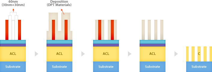
Double Patterning Tech. Materials
Due to delay of EUV(Extreme Ultraviolet) Lithography development and commercialization,
chipmakers had to choose DPT(Double Patterning Technology) process for wafer patterning
below 30nm. DPT process requires etch resistible layer materials such as DIPAS which is
deposited on top of a processed resist material to form sidewall spacers.
| Product |
Structure |
Property |
MSDS |
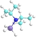
| DIPAS |
 |
Molecular Formula
Molecular Weight
Boiling Point
Vapor Pressure
Physical State/Color
Water Reactivity |
: C6H17NSi
: 131.30g/mol
: 117℃
: 55℃/106torr
: Colorless liquid
: Violently react |
|
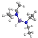
| E2S2 |
 |
Molecular Formula
Molecular Weight
Boiling Point
Vapor Pressure
Physical State/Color
Water Reactivity
|
: C8H22N2Si
: 174.40g/mol
: 188℃
: 25℃/0.795torr
: Colorless liquid
: Violently react
|
|